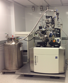
Zeiss ORION NanoFab HIM/FIB
Description
Please note: This tool is not included within a user package. Fee-for-Service is available at an hourly rate.
Zeiss’s ORION NanoFab multi-column (GFIS, and Gallium-FIB) Helium Ion Microscope (HIM) and Focused Ion Beam (Gallium-FIB) is designed for in-situ milling of most materials. The HIM beam is capable of providing sub 0.5 nm image resolution, with a beam energy range of 10 to 30 kV, and beam current range from 0.1 to 100 pA. The Gallium FIB column can provide sub 3 nm resolution at 30 kV, with beam energy from 1 pA to 100 nA.
The system contains an airlock chamber providing a sample exchange time of 3 min. It uses an Everhart Thornley secondary electron detector, and is also equipped with an electron flood gun for imaging non-conductive samples and materials. It is capable of producing 4k image sizes. The nanopatterning and visualization engine uses a 16 bit scan generator, and dual signal acquisition modules.
It also has a Gas Injection System (GIS), that can perform patterning depositions of tungsten (conductor), TEOS (insulator), and xenon difluoride (XeF2), which increases the etch rate of silicon.
Both HIM and FIB columns can do both milling and imaging. Imaging can be destructive. This tool is not easy to use; it requires many months of practice and experience. Anyone wanting to be trained on this tool will first need to complete all the prerequisites.
- Rating: 10/10
- Prerequisites:
- Evaporator
- AFM
- SEM
- EBL
- Spin processor
- Dektak
- Knowledge of Ion beam milling, pattern generators, CAD layouts
Download the ORION NanoFab Brochure (PDF version, 5.20 MB)